What Dane deQuilettes works on —
and where a self-improving lab could help
A short read, no science background needed. Dane's whole career runs on one idea: you can read a material's quality just by shining light on it — no wires, no waiting. He turned that into a solar-cell reputation, a way to grow world-class quantum diamond, and a measurement company. Each section is simple; open the grey toggles if you want the real detail.
Who he is
| Now | Assistant Professor at Princeton (Electrical & Computer Engineering), running a new lab on quantum and energy materials. |
| Known for | Some of the most-cited work in perovskites — the thin, cheap semiconductor that could make solar power far better. |
| Also | Grew some of the highest-quality quantum diamond ever made; co-founded a measurement startup, Optigon. |
| The idea behind it all | Light is a contactless voltmeter: how a material glows tells you how good it is, and how good a device it could become. |
More detail — background & record
~9,500 citations, h-index ≈ 26. B.S. Pepperdine → PhD at the University of Washington (David Ginger group, 2017) → postdoc at MIT (Vladimir Bulović, leading the Tata–MIT GridEdge solar program) → MIT Lincoln Laboratory (quantum diamond, ~2021–23) → Princeton (2026).
Co-founded Optigon (MIT spinout, 2021) and served as its Chief Science Officer through ~2025; the company is now run by his co-founders while he leads the academic lab. Named to Scientific American's inaugural "Young American Scientists" list (2026); Forbes 30-Under-30 (2020).
His core idea: read a material by its glow
Shine a light on a semiconductor and it glows back. Dane's insight, over a decade of work, is that the brightness and the way the glow fades are a precise report card: they reveal the hidden flaws that waste energy, and even the top voltage a finished device could reach — all without ever touching the sample.
His 2015 landmark was the first to map those flaws across a real perovskite film, showing the good and bad patches side by side. That reframed the whole field around fixing defects — and it's the thread running through everything he's done since.
More detail — the key perovskite papers
- Science, 2015 — "Impact of Microstructure on Local Carrier Lifetime" (~2,500 citations). Combined glow imaging with electron microscopy on the same spot; proved energy loss is patchy and tied to grain boundaries. The paper that pointed the field at defect engineering.
- Nature Photonics, 2018 — perovskite films glowing at >90% efficiency, near the theoretical limit — the benchmark for how good these materials can get.
- Nature Energy, 2024 — a surface treatment giving a carrier lifetime over 30 microseconds (billed the longest for any direct-bandgap semiconductor in 50 years) and solar cells above 25% efficiency.
- ACS Nano, 2025 — mapping how energy actually flows through the film (it moves ~29% faster in some directions than others).
Turning glow into a solar-cell predictor
Here's the payoff, and the part most relevant to us. Building a full solar cell is slow, and most experimental ones turn out mediocre — so you waste effort finishing duds. Dane's team showed you can predict how good the finished cell will be while it's only half-built: take three quick optical readings, run them through physics, and forecast the cell's voltage. Then you finish the winners and skip the losers.
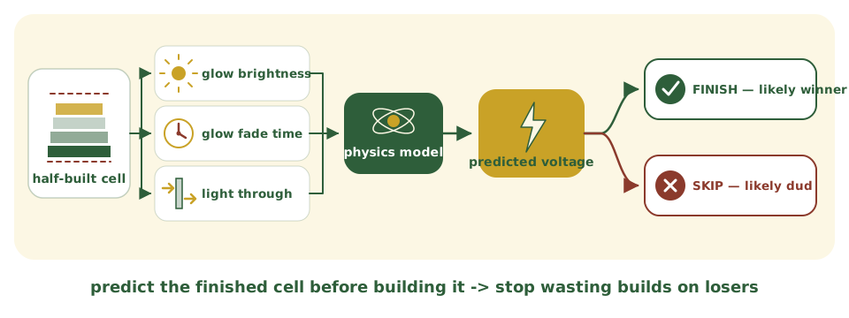
A "go / no-go" gate, before the expensive final build steps. Crucially it's physics-based, not a black box.
More detail — how it works, and its honest limits
Preprint arXiv:2508.21037 (an NREL–Optigon collaboration). Three non-contact measurements on half-fabricated devices — steady-state glow (→ light-emission efficiency), time-resolved glow (→ how fast energy is lost), and transmission (→ thickness/absorption) — feed a detailed-balance physics model that outputs an "implied voltage."
Tested on 120 device pads across process variations. It correctly ranks the conditions (it found that a specific hole-transport bilayer cuts voltage loss by >100 mV — the interface, not the absorber, is the differentiator). Honest limits: it's trend-level, with a consistent ~170 mV offset from the layers added after measurement, and no accuracy figure (R²/MAE) is published. The paper's own closing line asks to extend the model to predict current, fill factor, and full efficiency — not just voltage. That open ask is exactly a place a learning loop could help.
A different material entirely: quantum diamond
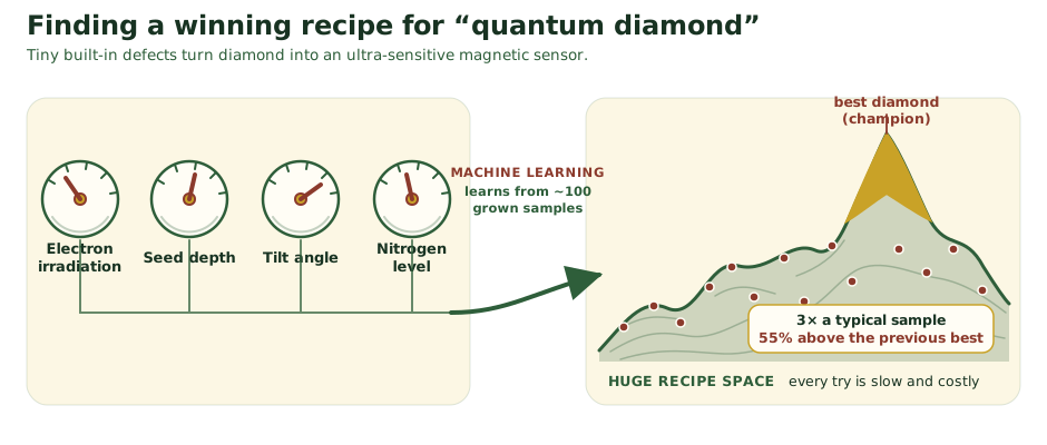
In a separate line of work (from his time at MIT Lincoln Lab), Dane grows diamond with tiny built-in defects that make it an ultra-sensitive magnetic sensor. Growing a great one means tuning a dozen knobs, and each attempt is a slow furnace run. His team let machine learning search the recipe space — and found a new sweet spot 3× better than a typical sample and 55% better than the previous best. The old champion took about two years of hand-tuning; the ML search took a few months.
More detail — the method & the physics it revealed
Preprint arXiv:2510.22121 (MIT Lincoln Lab; he's co-first author). The approach: compare several models (gradient boosting won), then use Bayesian optimization as an active-learning loop, with a tool called SHAP to see which knobs matter. Four dominated (~75% of the behavior): electron-irradiation dose, how deep the seed sits in the plasma, the seed's tilt angle, and the reactor's nitrogen level.
The physical payoff: nitrogen and irradiation dose have to be co-optimized — more nitrogen boosts the signal but wrecks the sensor's "memory" (coherence time), so the best recipe balances them, in a corner of the space nobody had explored. The winning window was validated by growing 18 new diamonds.
Where a self-improving lab could help
Notice the pattern across all three: a fast way to measure, and a slow, costly way to make. That gap is exactly what our team at Ohara Labs works on — a loop that proposes the next thing to make, measures it, and decides what to try next, reaching a target in far fewer expensive runs.
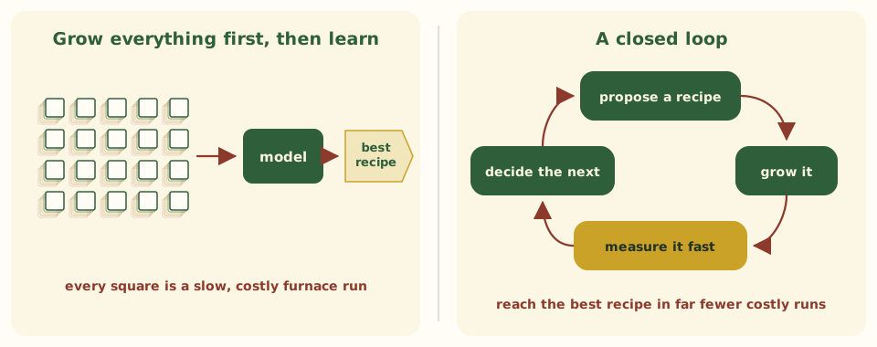
But "add machine learning" isn't the pitch — he already does that. Two things are more specific and more useful:
- Extend the half-built-cell predictor to full efficiency — the exact next step his paper asks for — so a go/no-go gate can retire likely losers before anyone finishes them. The quantity that drops is the number of full devices you have to build to find the winner.
- Close the loop on the recipe search — for diamond growth or perovskite surface treatments — cutting the number of costly runs to hit a target, with a fast measurement (his own tools are ideal for this) scoring each attempt.
To be clear: these are directions we'd explore together, not results — the "how much better" is what an experiment would measure.
The company he co-founded: Optigon
He didn't just publish the "read a material with light" idea — he turned it into a product. Optigon (an MIT spin-out, 2021) builds a benchtop instrument, Prism, that runs his lab techniques automatically: shine light, read the glow and the transmission, and get a material's quality — and a forecast of the device it could become — in milliseconds, without ever touching the sample. He co-founded it and was its Chief Scientist; it's now run day-to-day by his co-founders while he leads the Princeton lab.
Why it matters to us specifically: a self-improving lab is only as fast as its measurement. Prism is built to be that fast measurement — Optigon even markets it for "self-driving labs." It's the missing fast, honest oracle that a decision loop needs to sit on top of.
More detail — how Prism actually works
Three optical modes in a single non-contact head:
- Transmission (~20 ms) — how much light passes through → thickness and absorption.
- Steady-state glow / photoluminescence (~100 ms) → how efficiently the material re-emits light, a direct read on quality.
- Time-resolved glow (~100 ms, 0.5 ns resolution) → how fast energy leaks away (the non-radiative loss).
Selectable lasers (405–820 nm); maps a sample point-by-point down to tens of microns; scans up to a full G12 (210×210 mm) wafer, or dozens of small coupons, in seconds; controlled and analysed through a Python API — i.e. it's automation-native, not a manual GUI tool. From those optics it forecasts a finished cell's voltage, current and fill factor. (That forecasting is an emerging capability: today it's most reliable at ranking which process is better, with absolute accuracy still improving.)
More detail — the business (founders, funding, the market)
Founders (all out of MIT's GridEdge solar program): Anthony Troupe (CEO) and Brandon Motes (CTO), with deQuilettes as co-founder/Chief Scientist — both Troupe and Motes made Forbes 30-Under-30 in 2026. Based at Greentown Labs in Somerville, MA; team of roughly a dozen.
Funding is grant-based so far (no big venture round): about $1.3M from the US Department of Energy (SBIR Phase I + II) plus Massachusetts state grants — on the order of $1.5–2M total.
The market: they sell to three kinds of customer at once — university research labs, solar-cell manufacturers wanting in-line quality control, and automated ("self-driving") labs. Rivals tend to do one slice each — inline glow-imaging for silicon (pass/fail), or slow lab-grade time-resolved measurements — while Optigon's pitch is all of it at once, fast, non-contact, and scriptable. The strongest scientific competitor on raw accuracy is a tool called Photon etc's IMA, but it's slower and not built for automation.
The rest of his work
- Better solar materials. Much of his reputation is in figuring out why energy leaks out of perovskites at their surfaces, and how to plug those leaks — central to making cheap solar cells that last (his 2024 Nature Energy paper set records for how long energy survives in the film).
- Quantum + climate. His stated ambition is to bring quantum-grade materials to bear on clean-energy problems — building new "reactors" to grow these materials and new light-based probes to watch them form.